


From Standardized Legacy to Cost-Oriented Integration
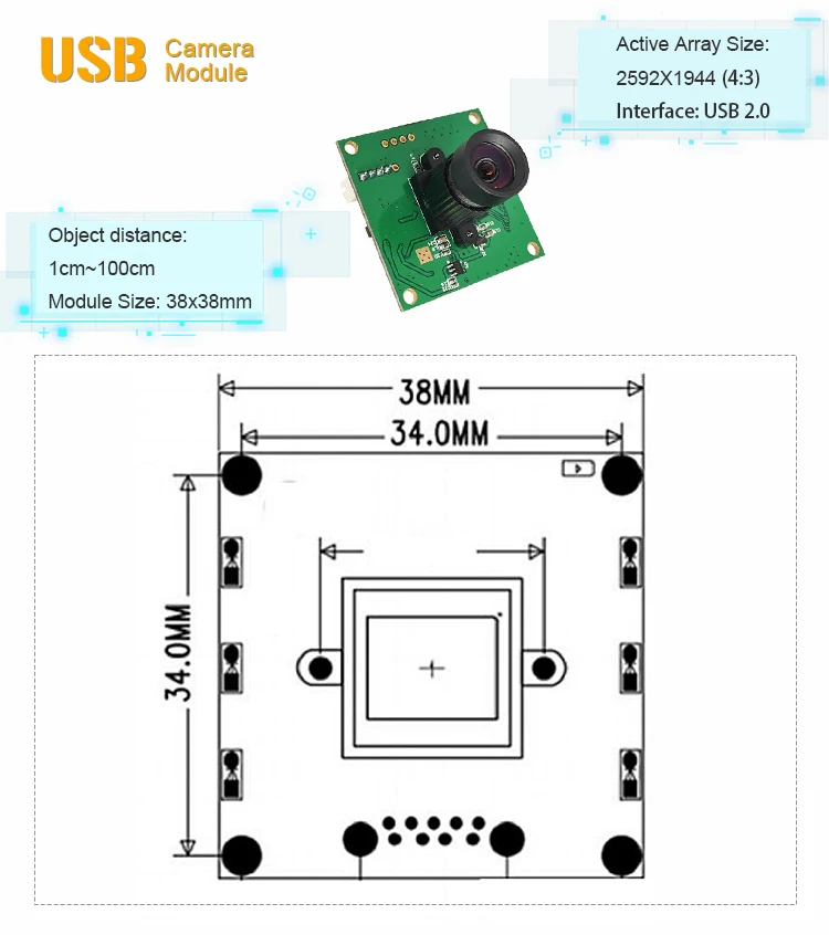
Although both the GalaxyCore GC5603 and OmniVision OV5640 are classified as 5-megapixel CMOS image sensors, they originate from fundamentally different technological generations and design philosophies. When evaluated at the camera module level, the distinction between them is not merely quantitative, but structural and strategic.
This analysis aims to clarify their respective advantages and limitations by examining pixel architecture, system compatibility, image quality stability, and long-term integration value.
I. Core Photosensitive Performance: A Game of Pixel Architecture and Light Efficiency
Photosensitive performance, determined by pixel size, photosensitive process, and signal processing technology, is the core competitiveness of image sensors. The two sensors adopt distinct design paths in this dimension.
The GalaxyCore GC5603 features a 1/2.7-inch optical format, a 2.0μm×2.0μm pixel size, and integrates Back-Side Illumination (BSI) technology. The larger pixel area significantly enhances the light-sensing capacity per pixel, and when combined with the optimization of the light-sensing path by BSI technology, it achieves superior Signal-to-Noise Ratio (SNR) in low-light environments and a wider dynamic range, effectively reducing highlight clipping and shadow detail loss. This characteristic enables the GC5603 to retain more details and deliver purer images in complex lighting scenarios such as night surveillance and in-vehicle low-light imaging.
The OmniVision OV5640 adopts a 1/4-inch (1/3.2-inch as noted in some documents) optical format with a 1.4μm×1.4μm pixel size, also equipped with the OmniBSI™ back-illuminated architecture. Although the smaller pixel size puts it at a disadvantage in light-sensing capacity per unit, the 2×2 pixel binning technology can increase the equivalent pixel size to 2.8μm, partially compensating for the low-light performance deficiency. It also supports 720P/60fps HD video recording with excellent in-frame detail sharpness. In addition, the OV5640 incorporates advanced digital noise reduction algorithms and Fixed Pattern Noise (FPN) suppression technology, maintaining a stable SNR of 46dB and outputting purer image signals under normal lighting conditions.
Notably, the GC5603's RAW output format is more suitable for professional module solutions requiring post-image optimization, while the OV5640 supports multiple output formats including RGB, YUV, and JPEG. Its integrated JPEG compression engine reduces the bandwidth pressure of module data transmission, making it more compatible with simple terminals requiring high real-time performance.
II. Module Integration and Adaptability: Size, Interface, and Flexibility
The miniaturization, integration complexity, and compatibility of camera modules are directly affected by sensor packaging and interface design, where the two products have different focuses.
The GC5603 adopts Chip Scale Package (CSP) with a single MIPI interface. Its compact packaging size meets the requirements for ultra-thin and miniaturized module designs, especially suitable for terminal devices sensitive to space, such as smartphone secondary cameras, smart wearables, and micro security cameras. The simplified interface design reduces module wiring difficulty, helping to improve mass production yield and control overall costs.
The OV5640 offers multiple packaging options including CSP-71p, BGA, and LCC, with excellent interface compatibility. It supports dual-interface modes of MIPI CSI-2 and Digital Video Port (DVP). This design allows it to adapt not only to mainstream smart devices but also to traditional embedded systems (such as Arduino and Raspberry Pi), gaining advantages in scenarios requiring high interface flexibility, such as industrial inspection and in-vehicle rearview imaging. Furthermore, the OV5640 integrates Auto-Focus (AF), anti-shake engine, and multi-zone automatic exposure control, reducing the need for external module components, simplifying integration processes, and shortening time-to-market.
However, the OV5640's multiple interfaces and integrated functions result in slightly higher power consumption than the GC5603. The GC5603's energy efficiency advantage is more prominent in low-power IoT terminals without external power supply.
III. Power Consumption and Reliability: Key Thresholds for Scenario Adaptation
For battery-powered or long-term operation terminals (such as security cameras and IoT sensors), power consumption and operational stability are core considerations for module selection, where the two sensors demonstrate complementary performance.
The GC5603 takes low power consumption as its core advantage. By optimizing the circuit architecture and working modes, it effectively controls energy consumption while ensuring 30fps full-resolution output, making it particularly suitable for low-power IoT terminals requiring long-term standby. Although its wide temperature adaptability is not explicitly labeled as industrial-grade, the heat dissipation advantage brought by its miniaturized packaging enables stable operation in enclosed modules.
The OV5640's power consumption is strongly related to its working mode. Under normal operation (30fps@VGA resolution), its power consumption is approximately 336mW. It also supports multiple low-power modes such as standby (<10μA) and sleep (≈100μA), allowing dynamic adjustment through software to balance performance and energy consumption. More notably, its operating temperature range covers -30°C to +85°C, meeting the rigorous requirements of industrial and in-vehicle scenarios. With excellent Mean Time Between Failures (MTBF) performance, its long-term operational stability has been verified in numerous practical applications. In addition, the OV5640 features mature power sequencing control and ESD protection design, reducing the failure risk of modules in complex circuit environments.
IV. Selection Decision: Scenario-Oriented Adaptation Logic
The differences in advantages and disadvantages between the two sensors essentially correspond to the needs of different module application scenarios. With larger pixels, low power consumption, and miniaturized packaging, the GC5603 is more suitable for terminals requiring high low-light imaging quality, space constraints, and battery power supply, such as smart wearables, micro security cameras, and low-power IoT terminals. The OV5640, with its core competitiveness in interface flexibility, rich integrated functions, and industrial-grade reliability, is more suitable for industrial inspection, in-vehicle imaging, embedded development projects, and multi-scenario module solutions requiring rapid mass production.
In terms of cost, the GC5603 has certain competitiveness relying on simplified function design and localized supply chain advantages. The OV5640, with its mature technical ecosystem, abundant development materials, and mass production experience, can reduce module design and debugging costs, making it suitable for projects requiring high stability and development efficiency.


